
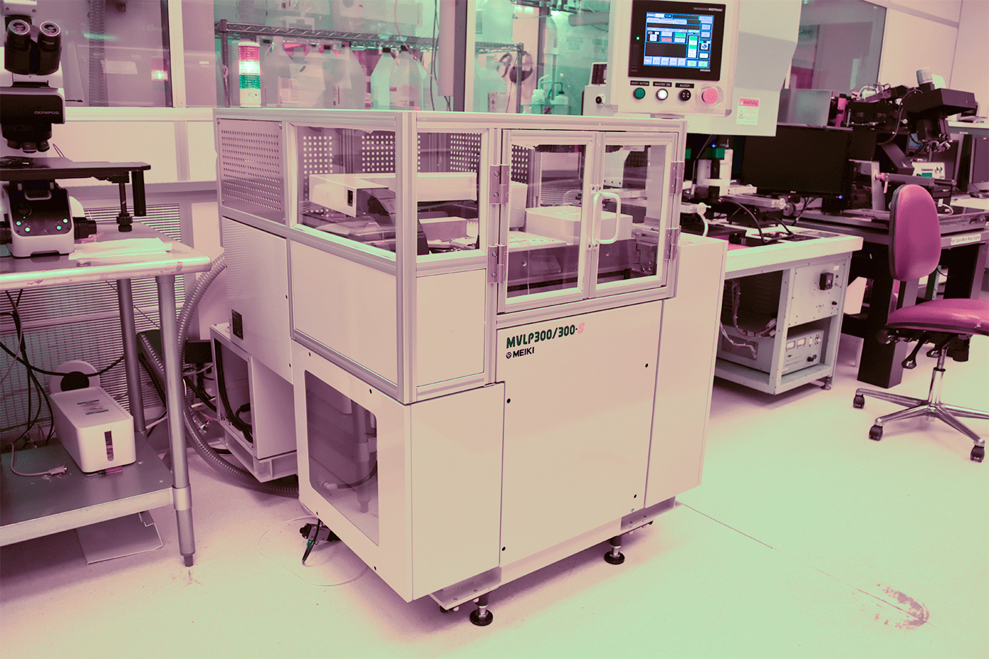
Dielectric Build-Up and Photoresist Processing
IMS provides advanced packaging capabilities, including dielectric build-up and photoresist processing with vacuum laminators, roll laminators, and spin coaters. Supporting substrates up to 300 mm, we enable die embedding and via-in-via dielectric formation with cutting-edge lamination technology.
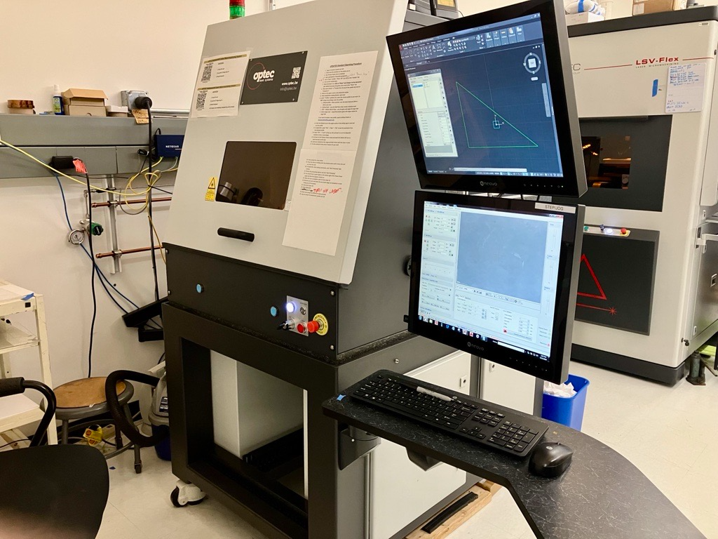
Micro-vias and Glass Cavities Formation
IMS's advanced packaging facility uses UV picosecond and femtosecond lasers for high-precision drilling, microvia formation, and glass cavity creation for die embedding. Supporting panels up to 300 mm, these systems deliver submicron accuracy, with Bessel lens tech for superior glass cavity fabrication.
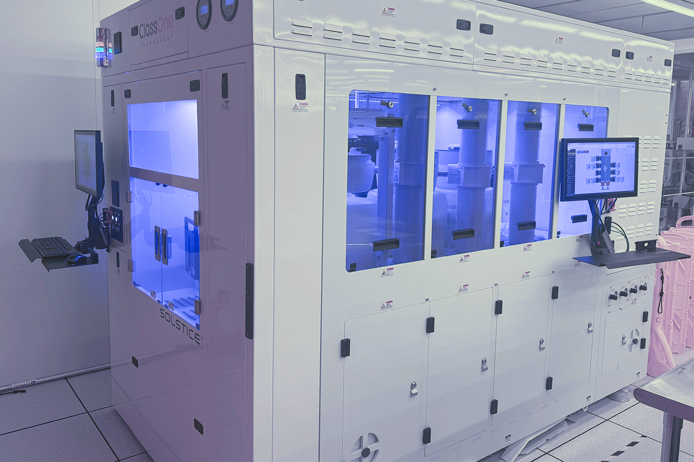
Metallization
IMS offers advanced metallization for packaging with a 300 mm plating line for conformal plating, microvia metallization, and through-hole filling. A new 8-chamber tool supports 4- and 8-inch wafers, enabling RDL plating, TSV copper fill, gold, NiW, and SnAg plating—all in one platform.
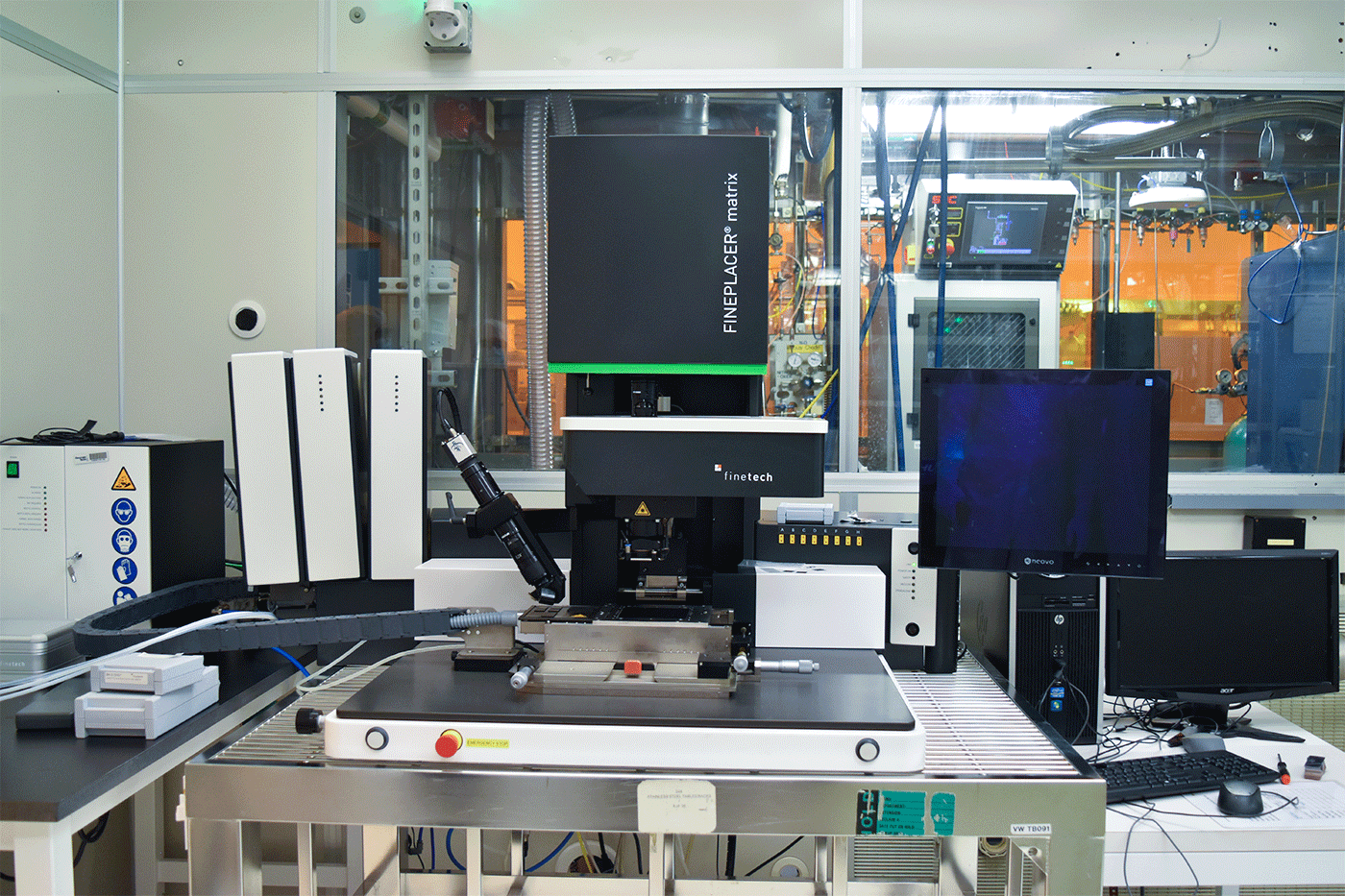
Bonding and Reflow
IMS provides advanced chip bonding and reflow for semiconductor packaging with tools like TPT HB100 wire bonder, Finetech Sigma and Matrix flip-chip bonders, BTU 8-zone and LPKF nitrogen ovens, plus precision screen printing—delivering flexible, reliable bonding solutions.
Environmental Testing and Reliability
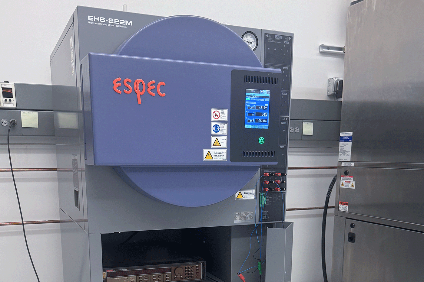
IMS offers environmental and reliability testing ovens for samples up to 300 mm, supporting HAST, thermal cycling, thermal shock, and liquid-to-liquid shock. All systems meet JEDEC standards, ensuring high-quality testing for durability and performance under extreme conditions.
Planarization, Grinding and Singulation
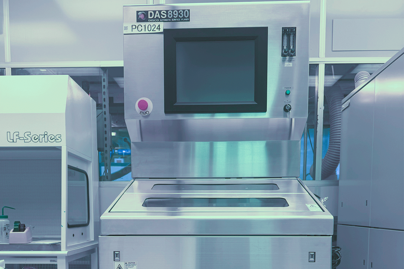
IMS offers wafer thinning, dicing, planarization, and CMP for advanced packaging. Supporting materials up to 300 mm, including glass, silicon, SiC, and sapphire, these capabilities enable 3D integration, MEMS, flexible electronics, and chiplet/SiP assembly with precision.
Failure Analysis and Characterization
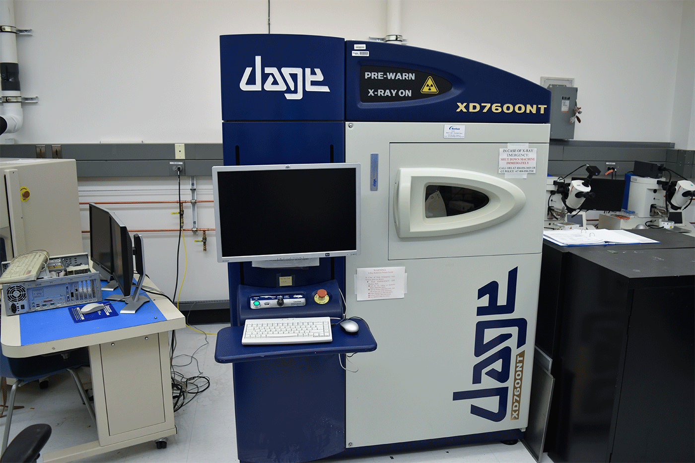
IMS offers advanced tools for surface analysis, failure inspection, and reliability testing, including 3D profiling, defect detection, warpage analysis, X-ray imaging, bond and peel testing, chemical analysis, and sub-THz antenna characterization—ensuring precision and performance.
Lithography
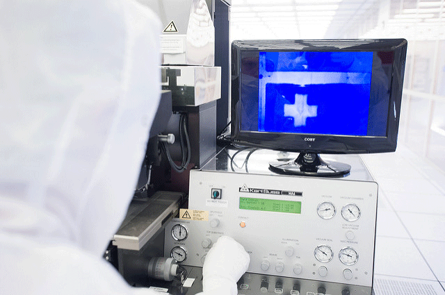
IMS offers advanced lithography tools for micro- and nanofabrication, including Elionix ELS-G100 e-beam, Heidelberg MLA maskless aligners, and SUSS MA6/MA8 mask aligners. These systems enable high-resolution patterning for semiconductors, MEMS, photonics, and quantum devices.