Scanning Probe Microscopy (SPM) instruments use a physical probe to scan and image the surface of a sample. The resolution of the microscope is not limited by diffraction, but only by the size of the probe-sample interaction volume, which can be as small as few angstroms. Unlike electron microscopy the specimen does not require vacuum and can be observed in air at standard conditions though vacuum and cryogenic temperatures are needed to achieve the highest resolution which can be a few picometers. This technique can measure 3D surface topography (x, y, and z dimensions), roughness, hardness, elasticity modulus, electrical properties, etc
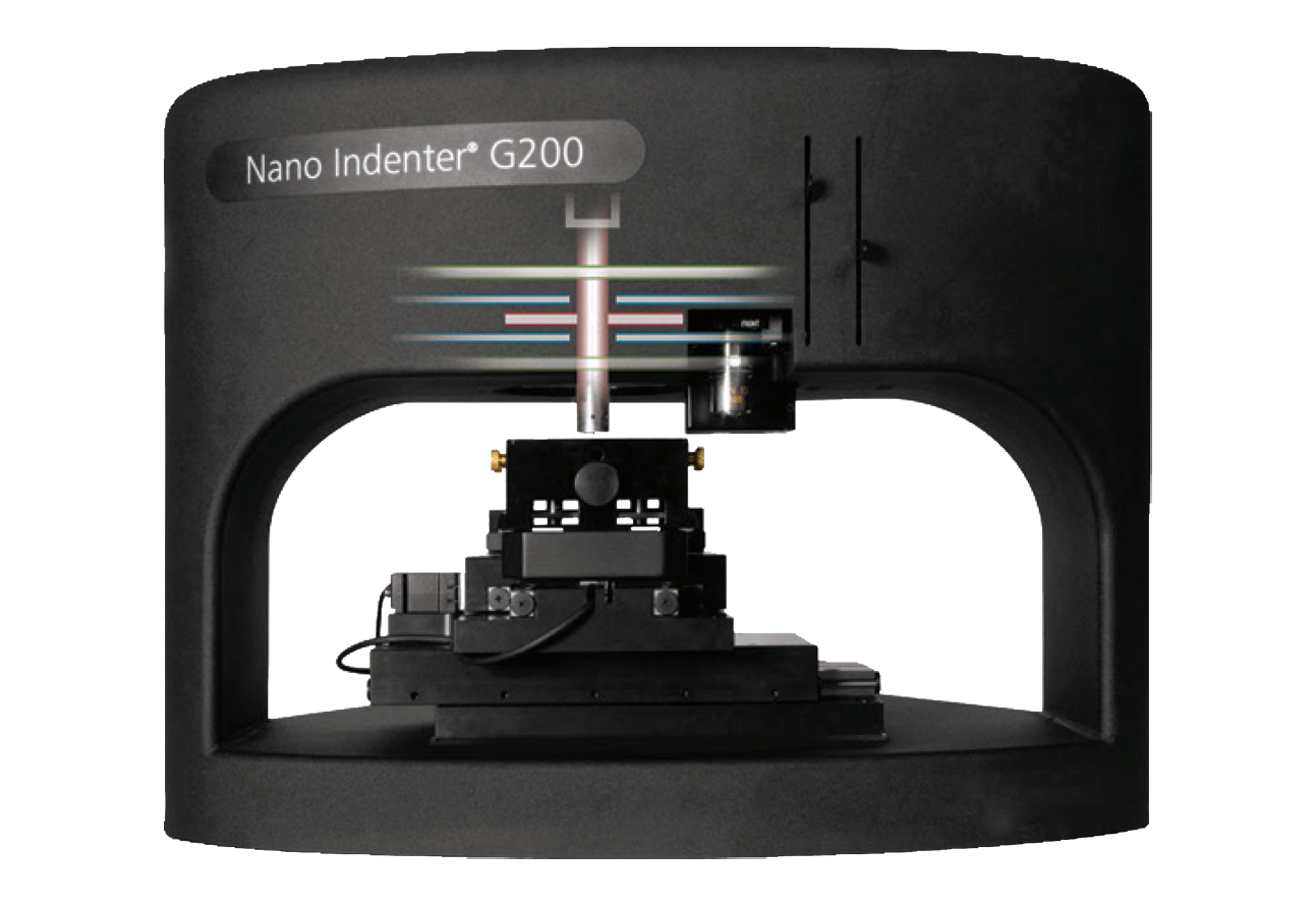
Agilent G200 Nanoindenter
The G200 nanoindenter enables users to measure Young's modulus and hardness in compliance with ISO 14577. The electromagnetic actuation allows unparalleled dynamic range in force and displacement control.
Bruker Dimension Icon AFM
The Bruker Icon Scanning Probe Microscope (SPM) system has a multitude of Atomic Force Microscopy (AFM) modes (e.g., AFM, PeakForce imaging, KPFM & cAFM, MFM, etch) to probe -respectively - dimensional, mechanical, electronic, magnetic, and other properties on the nanoscale down to the atomic scale.
Bruker Dimension Icon AFM-IR
The Bruker Icon-IR Scanning Probe Microscope combines atomic force microscopy with InfraRed laser spectroscopy to produce nano-scale chemical maps and FTIR-like spectra.
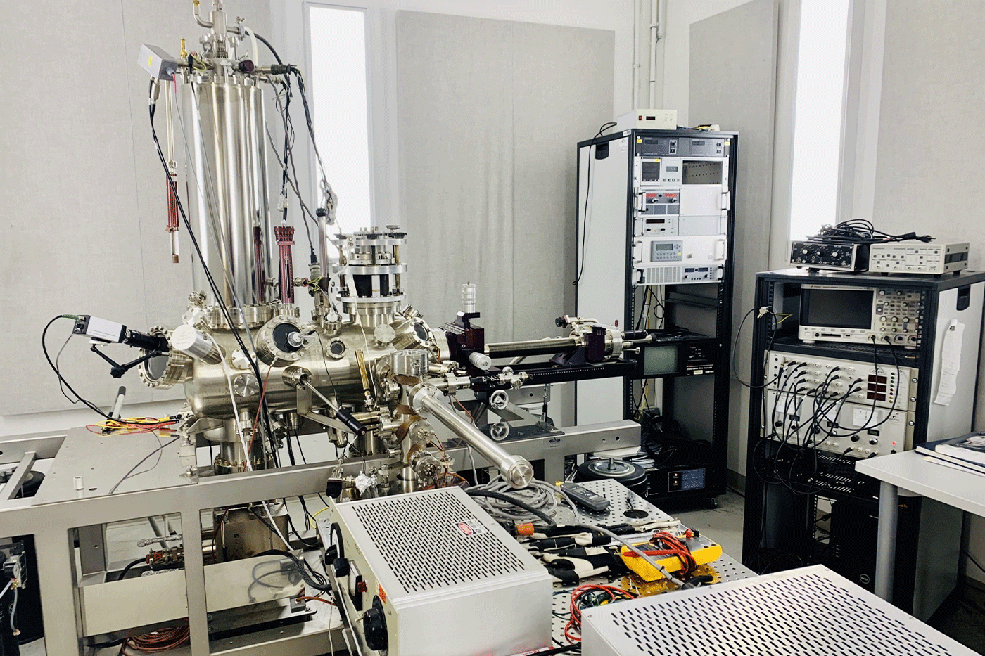
Createc LT-SPM
This Low-Temperature Scanning Probe Microscope (LTSPM) is one of few such tools available in a user facility in the U.S. The tool features a vacuum chamber that is as cold and empty as outer space with a module that allows scientists to image, experiment on, and even pick up and move individual atoms and molecules.
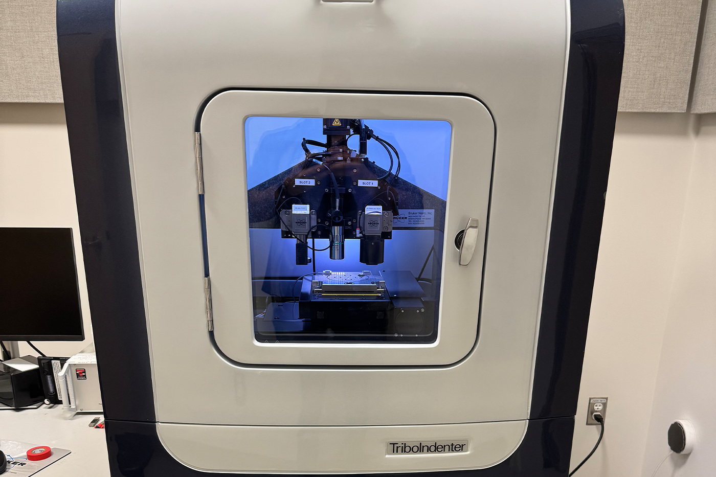
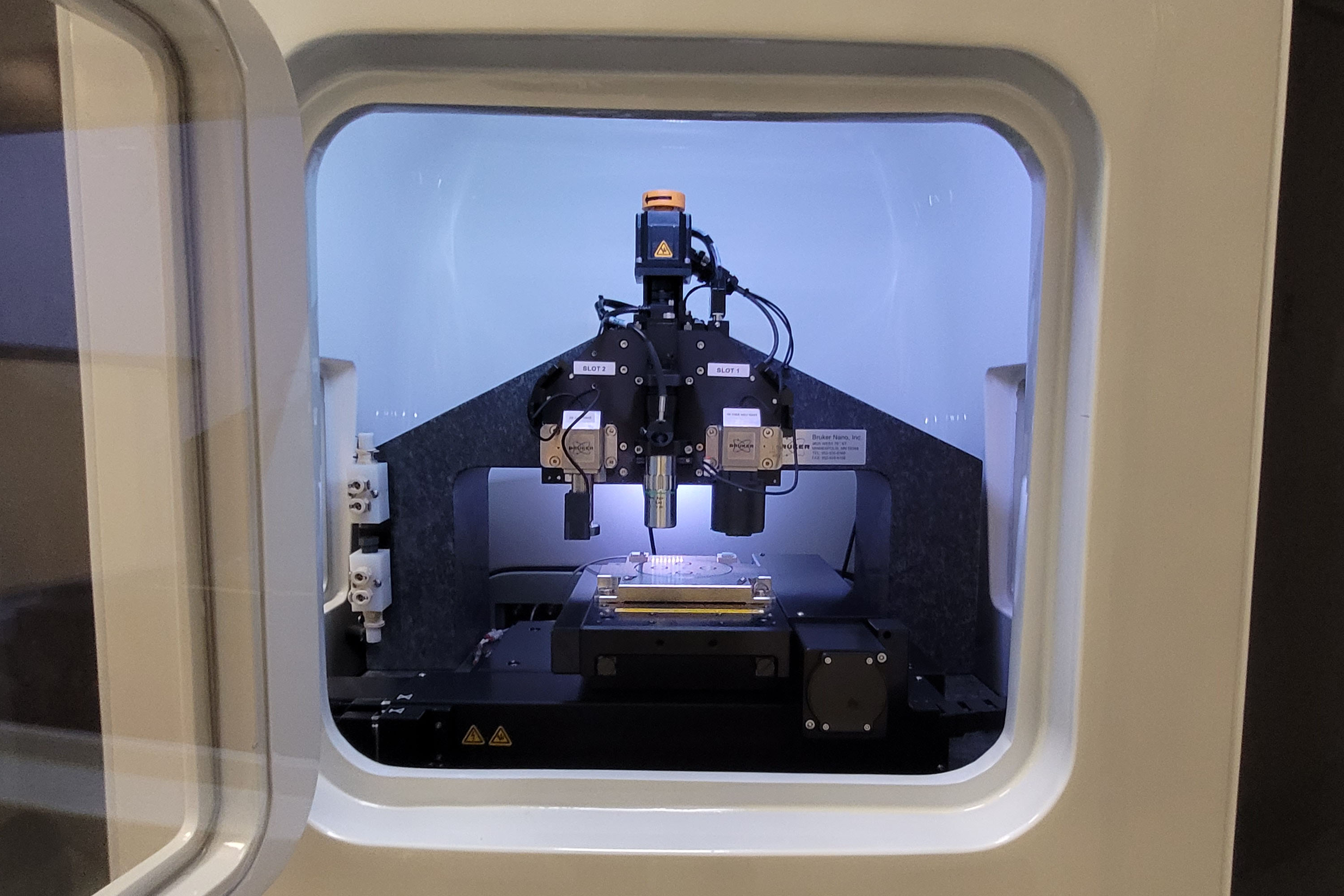
Hysitron TI-980 Triboindenter
The Bruker TI-980 triboindenter measures the hardness, modulus and other mechanical properties of micro-to-mesoscale, structures, thin films, and coatings.
Hystrion TI-900 Nanoindenter
The Hysitron TI-900 nanoindenter measures the hardness, modulus and other mechanical properties of micro-to-mesoscale, structures, thin films, and coatings.
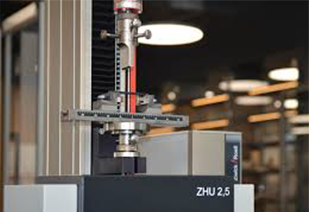
Zwick ZHU 2.5 Microindenter
The ZHU 2.5 microindenter is used to measure the hardness, modulus and other mechanical properties of meso-to-macroscale structures and coatings.