The IMS cleanroom at Georgia Tech offers advanced materials growth capabilities, including various Chemical Vapor Deposition (CVD) techniques. These include the growth of silicon-germanium nanowires, sulfurization growth, and the deposition of high-quality carbon nanotubes, carbon nanoribbons, and graphene thin films using Plasma-Enhanced CVD (PECVD). The facility supports substrates up to 4 inches and enables low-temperature growth, essential for producing single-wall and multi-wall carbon nanotubes and other nanomaterials.
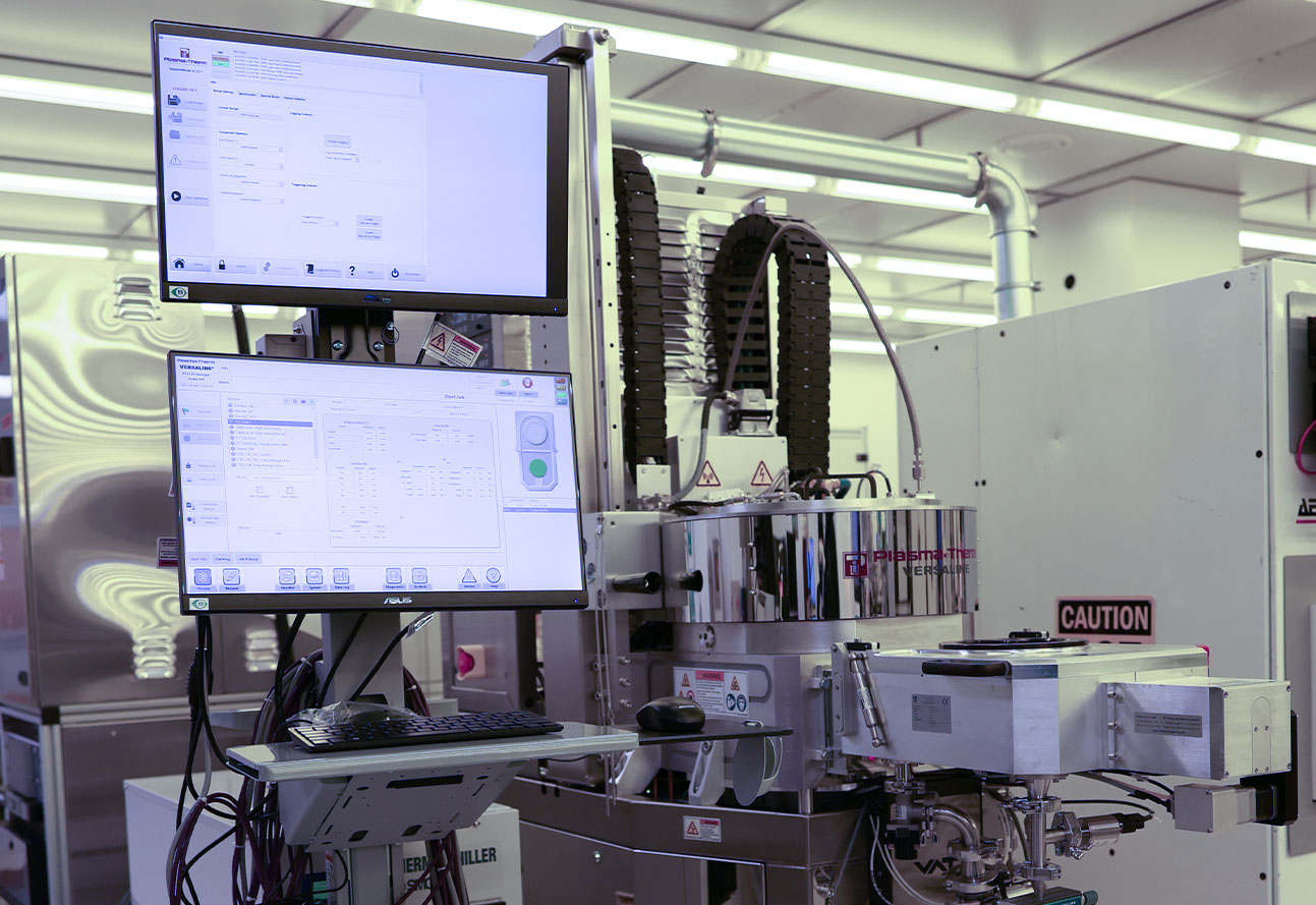
Plasma-Therm HDPCVD
The Plasma-Therm Versaline high density plasma chemical vapor deposition (HDPCVD) system uses an inductively coupled plasma to remotely ionize deposition molecules at high power away from the substrate. It then draws the ionized molecules to the substrate surface at low energy which reduces surface temperature while producing a high-density film. This technology provides a low temperature alternative to furnace driven processes and conventional plasma enhanced chemical vapor deposition methods for the deposition of silicon dioxide, and silicon nitride. The HDPCVD system produces high quality, pinhole-free films that are comparable to high temperature furnace deposited films. The system can accommodate substrates ranging from 200 mm diameter wafers down to small pieces. The HDPCVD configuration provides a process route to more dense films with lower wet etch rates at temperatures lower than 150C. This lower temperature makes deposition possible for applications with thermal budgets that exceed what PECVD can deliver. With the added capability of substrate bias, trench fill is possible, along with more planarized films on patterned substrates.
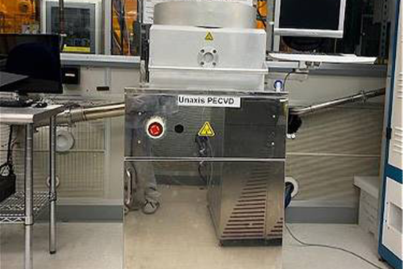
Unaxis PECVD
The Unaxis PECVD is an open chamber Plasma-Enhanced Chemical Vapor Deposition (PECVD) equipment for deposition of high-quality semiconductor and dielectric thin films. The tool is equipped with SiH4, N2O, NH3, PH3, B2H6 processing gases. It can deposit SiO2, SiN, low-stress SiN, SiON, a-Si, p/n doped a-Si. The 12-inch platen allows up to four 4in wafers to be processed simultaneously. The max temperature supported is 400C on platen.
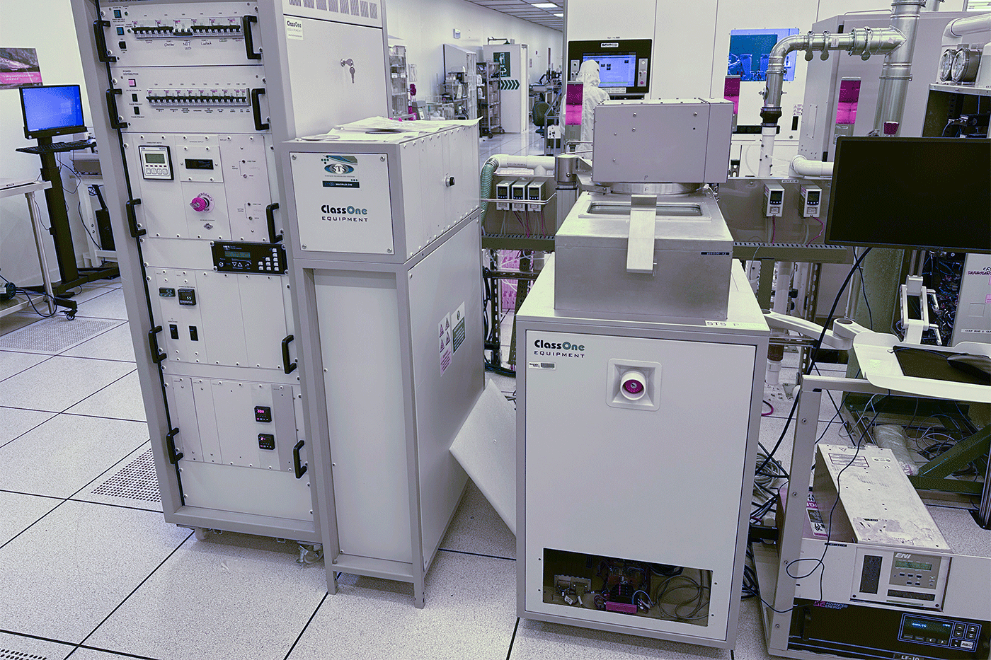
STS PECVD
The STE PECVD 3 is a closed chamber Plasma-Enhanced Chemical Vapor Deposition (PECVD) equipment for deposition of high-quality dielectric thin films. The tool is equipped with SiH4, N2O, NH3 processing gases. It can deposit SiO2, SiN, low-stress SiN. The tool is equipped with load lock which allows two 4in wafers to be loaded at same time, which only 1 wafer will be processed each time. Small pieces can be loaded in Al tray for processing. The max temperature supported is 400C on platen
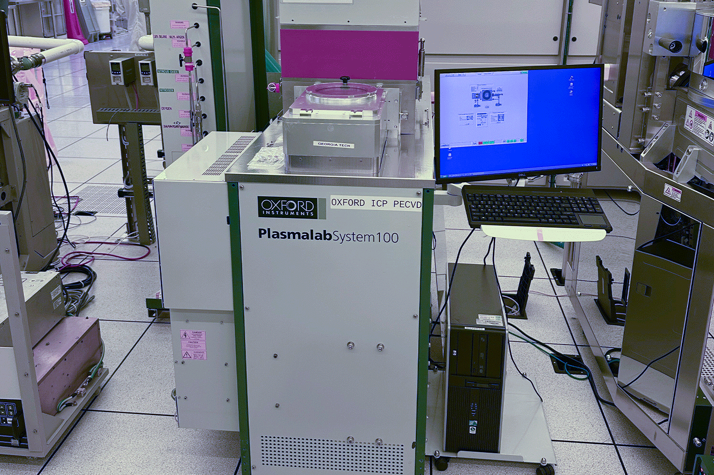
Oxford ICP-PECVD
Oxford ICP-PECVD systems are used for depositing high-quality dielectric films at low temperatures with low damage, utilizing high-density plasmas. The Oxford PlasmaLab System100 is used for materials such as SiO2, Si3N4, and SiON, and DLC. It features an ICP-source with SiH4/NH3/N2 for nitride and SiH4/N2O/N2 for oxide deposition. The standard recipes deposit films at 100C (up to 300C) and it can also deposit films at room temperature. The deposit film has
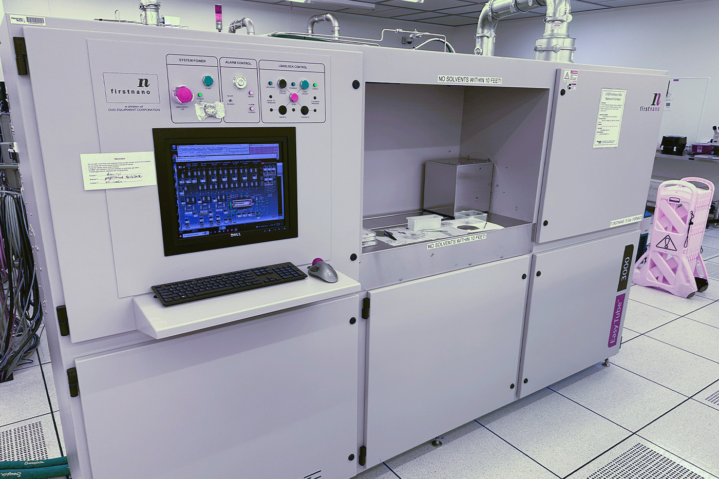
CVD FirstNano SiGe Nanowire Furnace
The Georgia Tech SiGe Nanowire furnace is configured for depositing Si nanowires from metal nanoparticles such as Au. Substrate material is typically Si. Samples are heated via infrared lamps from top and bottom.
Specifications:
- 350C - 900C
- SiH4, H2, Ar, Ge, 0.1% PH3
- base pressure 1e-3 Torr
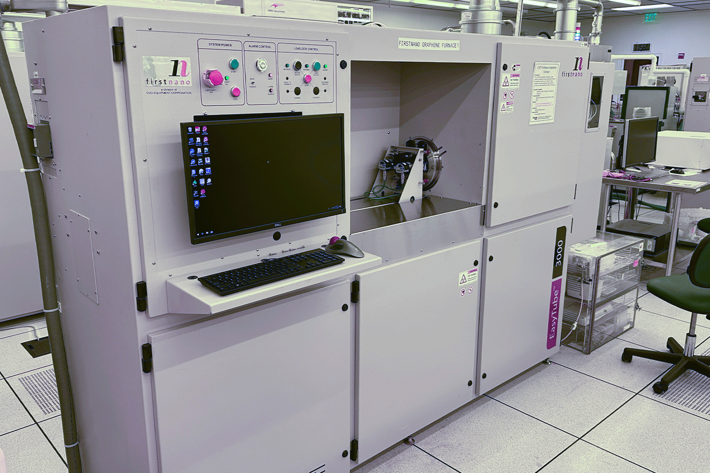
CVD FirstNano Graphene Furnace 1
The Georgia Tech CVD FirstNano Graphene furnace is currently configured for graphene on Cu foil, graphene sublimation from SiC samples (epitaxial graphene), and H2 etch clean of samples. Samples are heated via 10kW RF induction heating.
Specifications:
- quartz chamber with graphite susceptor
- 3in wafer and small pieces
- 2200C max
- fully programmable
- turbo pump for low pre-processing base pressure (9.0e-7 Torr)
- Ar, H2, SiH4, CH4
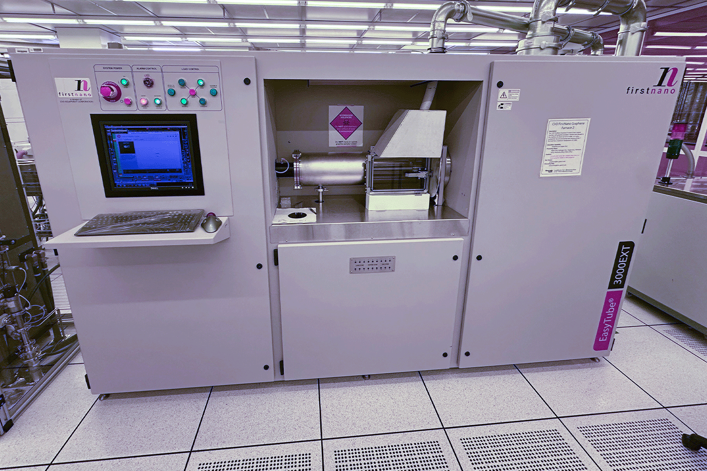
CVD FirstNano Graphene Furnace 2
The Georgia Tech CVD FirstNano Graphene furnace is currently configured for graphene on Cu foil, graphene sublimation from SiC samples (epitaxial graphene), and H2 etch clean of samples. Samples are heated via 10kW RF induction heating.
Specifications:
- quartz chamber with graphite susceptor
- 3in wafer and small pieces
- 2200C max
- fully programmable
- turbo pump for low pre-processing base pressure (9.0e-7 Torr)
- Ar, H2, SiH4, CH4
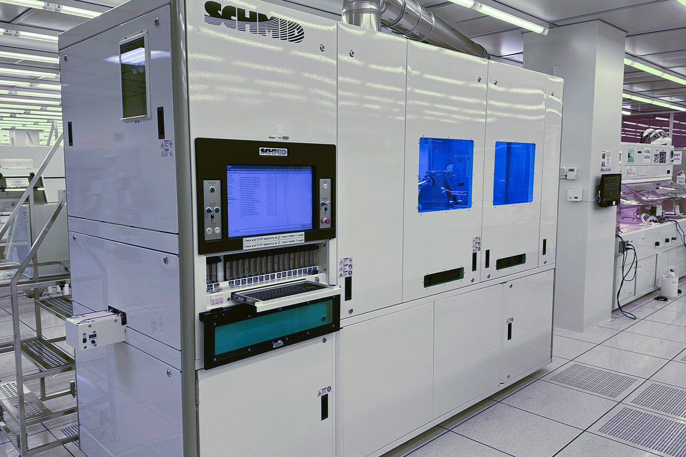
Schmid APCVD
The Schmid APCVD system is well suited for low-cost high-volume processing for all cell architectures requiring single or multi-layer dielectric thin film deposition. This is a roll-to-roll processing tool. Its horizontal inline design ensures that each substrate receives the same process treatment resulting in excellent layer uniformity. Depositing single-sided and therefore highly efficient.
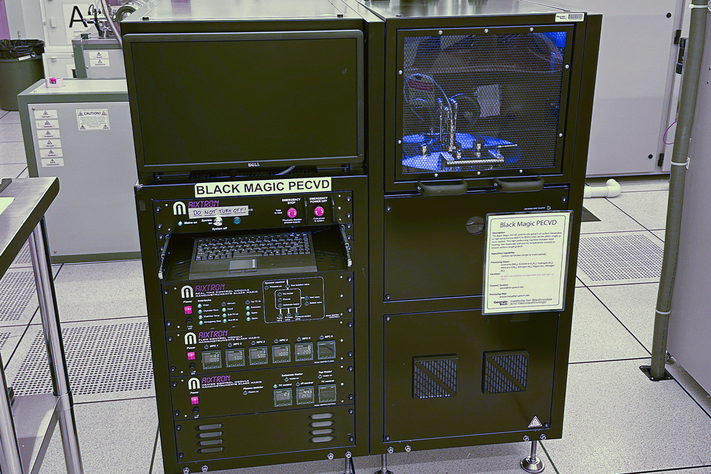
Black Magic PECVD
The Georgia Tech Black Magic PECVD system is a Plasma-Enhanced Chemical Vapor Deposition (PECVD) tool designed for the high-quality deposition of carbon-based nanomaterials, including carbon nanotubes (CNTs) and carbon nanoribbons (CNRs). The system supports the growth of both single-walled and multi-walled CNTs, with the outcome determined by specific process parameters. This system is well-suited for low-temperature deposition applications and can accommodate substrates up to 4 inches in diameter, typically silicon wafers capable of withstanding the required processing temperatures. A wide range of pre-loaded recipes are available, including specialized CNT "supergrowth" processes that enable rapid and vertically aligned CNT growth. Depending on the selected parameters and desired material properties, the deposition process can be completed within minutes. Under optimal conditions, CNTs can grow to several microns in length, and in some cases, even exceed one millimeter.
LPCVD

Tystar Nitride 4
The Georgia Tech Tystar Nitride Furnace 4 is used for LPCVD silicon nitride, including stoichiometric silicon nitride and low stress silicon nitride. Common recipes: NITRCOMM.004, LSNITRID.004 (Deposition rate: 3.46 nm/min, n=2.28), with the process temperature at 800C and 830C, respectively. The stoichiometric silicon nitride can be also processed at 770C to allow hydrogen free films. Max process temperature that tool allows is 850C.

Tystar Poly 3
The Georgia Tech Tystar Poly Furnace 3 is used for polysilicon deposition at a low pressure and low temperature with silane (SiH4). The common process, Polysi.007, is run at 250 mT and 588C. It can also run at lower temperature, such as 530C, for more amorphous structure, or higher temperature, such as 625C, for more crystalline structures. Doped silicon film can be made with the doping gas, phosphine (PH3). Max process temperature is 750C.

Tystar Poly 4
The Georgia Tech Tystar Poly Furnace 4 is used for polysilicon (undoped and P-doped) deposition at a low pressure (250 mT) and low temperature (588C) with silane (SiH4) and diborane (B2H6). Common process recipes: POLYCOM.008 BDPOLY.008 STBY.008 Max process temperature is 750C.
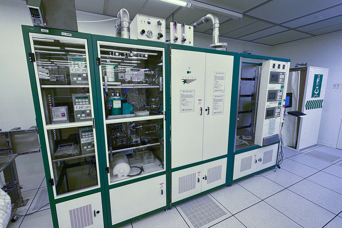
Tystar Mini 3
The Georgia Tech Mini Tystar 3 (mini Tystar 4600) is used for low temperature oxidation (LTO) at 725°C and pressure of 300mT. Batches of 4” silicon wafers (up to 25 wafers) can be processed at the same time, and the oxide uniformity is usually less than 3%.
Tempress Furnace 1 (POCl3)
The Tempress Low Pressure Chemical Vapor Deposition (LPCVD) system is a modular horizontal furnace designed to process substrates up to 150mm in diameter as part of the semiconductor, optical, MEMS, and solar device manufacturing. It is a 4-stack system set up to deposit silicon nitride, polysilicon, low temperature oxide (LTO), silicon rich oxide (SRO), phosphorus doped LTO, and phosphorus doped polysilicon. All tubes operate independently.

Tempress Furnace 2 (BBr3)
The Tempress Low Pressure Chemical Vapor Deposition (LPCVD) system is a modular horizontal furnace designed to process substrates up to 150mm in diameter as part of the semiconductor, optical, MEMS, and solar device manufacturing. It is a 4-stack system set up to deposit silicon nitride, polysilicon, low temperatrue oxide (LTO), silicon rich oxide (SRO), phosphorus doped LTO, and phosphorus doped polysilicon. All tubes operate independently.