Two small precision-cut metal gears with intricate spokes and teeth are displayed against a light background, illustrating microscale fabrication or machining.

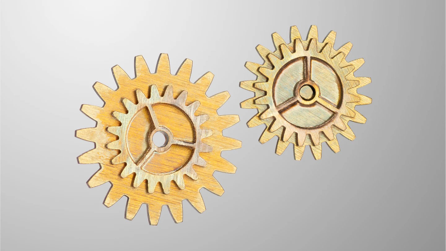
Example of micropart cutting and welding using a single source


Scanning electron microscope (SEM) images show a textured titanium alloy surface with layered microscale patterns created by laser irradiation, including a magnified inset highlighting fine surface features and scale measurements.  Close-up of a metal cardiovascular stent with an intricate lattice structure mounted on a catheter against a dark background.  Scanning electron microscope (SEM) images show cross-sectional views of layered material structures with visible fracture patterns and delamination featu

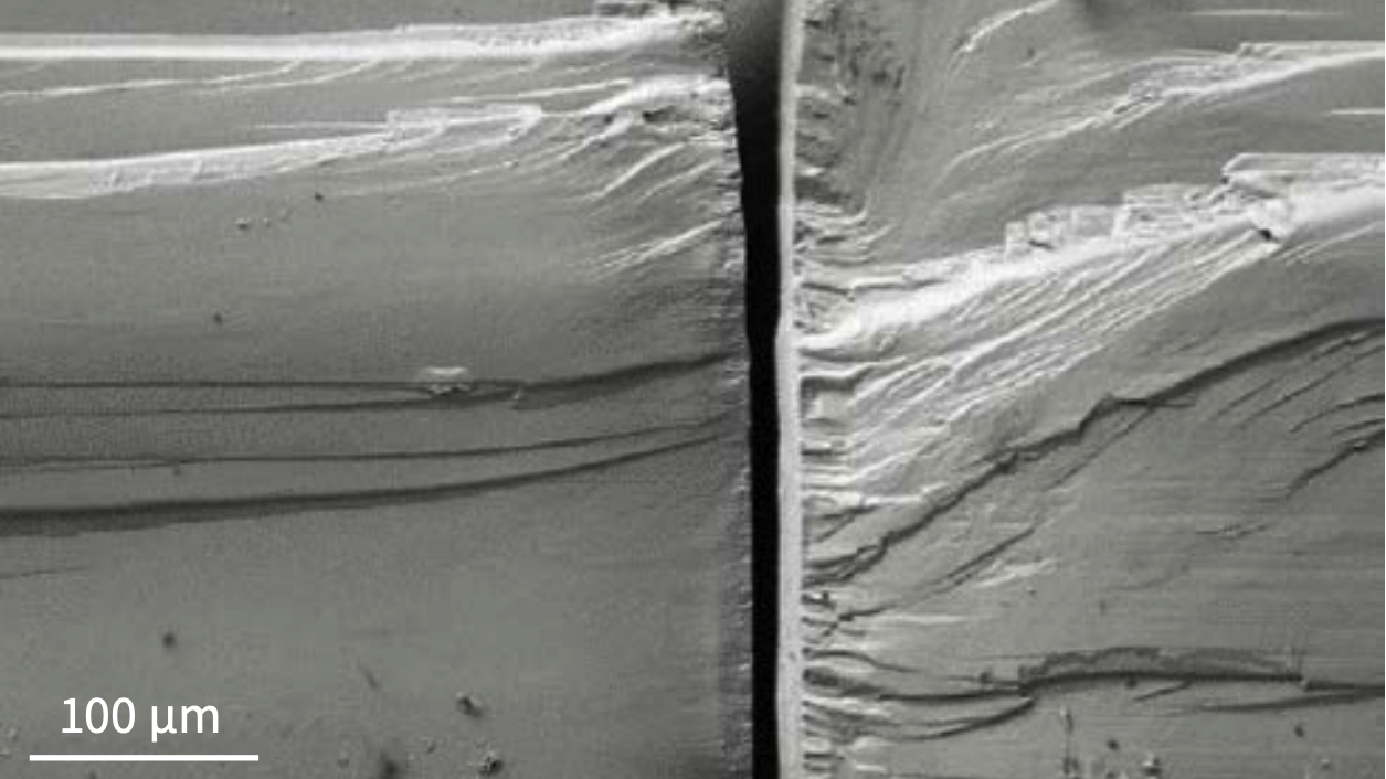
Brittle and highly thermally sensitive material cutting. 

Courtesy of Micronanics Laser Solutions Center.

Scanning electron microscope (SEM) images show a textured titanium alloy surface with layered microscale patterns created by laser irradiation, including a magnified inset highlighting fine surface features and scale measurements.

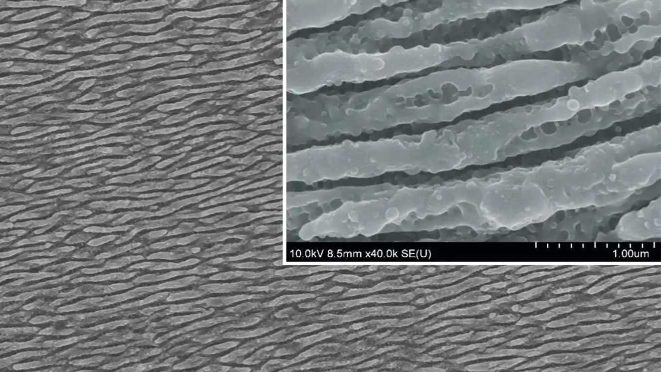
SERS sensor fabrication.​

Source: Nanomaterials (2019).

Scanning electron microscope (SEM) images show a textured titanium alloy surface with layered microscale patterns created by laser irradiation, including a magnified inset highlighting fine surface features and scale measurements.  Close-up of a metal cardiovascular stent with an intricate lattice structure mounted on a catheter against a dark background.

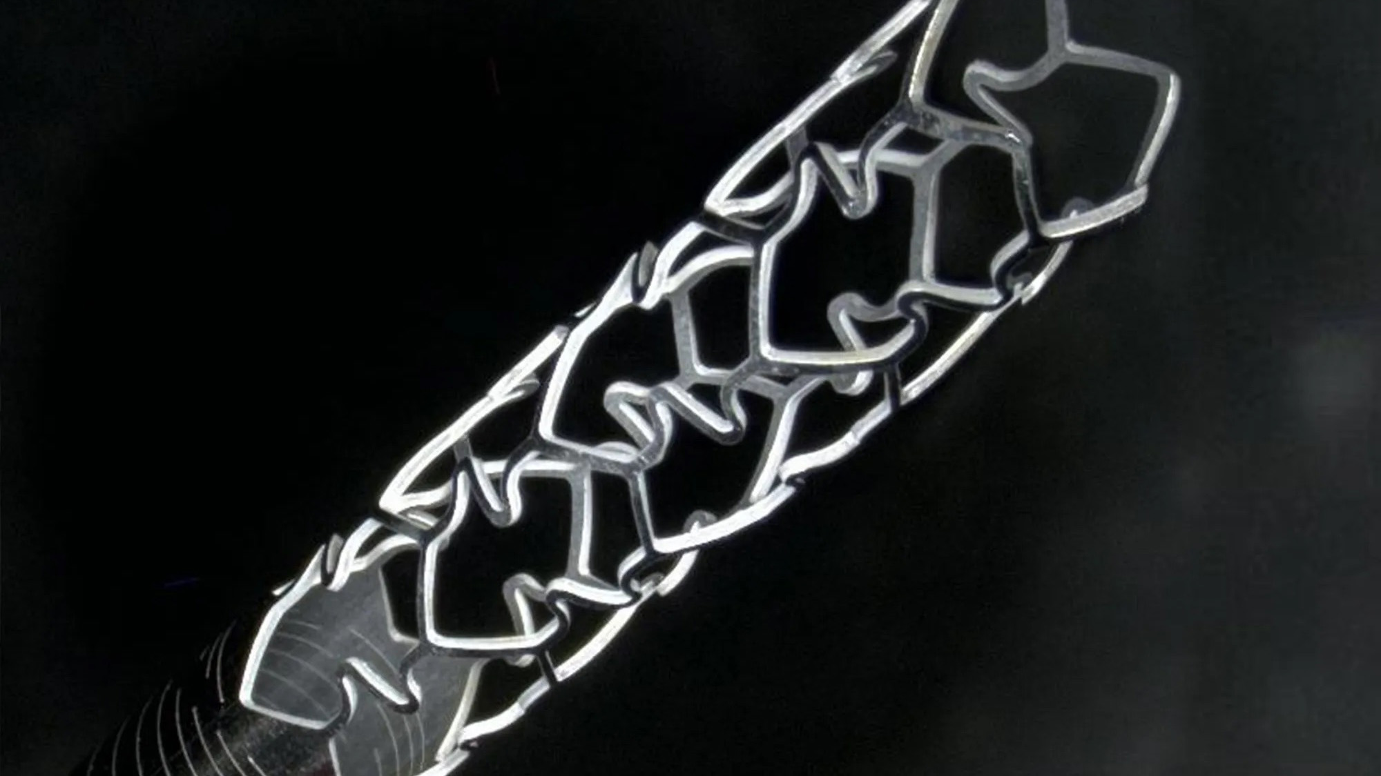
Stainless steel stent cutting.​

Courtesy of Amada Miyachi America.

Micromachining Applications​

  • Metal processing​

  • Selective ablation​

  • High contrast marking​

  • Volume modification​

  • Polymer processing​

  • Brittle material processing​

  • Transparent material processing​

  • Glass cutting and drilling​

  • Gasoline injector nozzle drilling

  • Dicing of LED/electronics chips​

  • Hard material processing for tooling​

  • Glass/Sapphire cutting​

  • Polymer material cutting​

  • Heat sensitive ceramic scribing​

  • LCD/OLED repair and cutting​

  • VIA drilling​

  • Probe card hole drilling/pin formation​